Advanced packaging: Applied and Intel widen their chipmaking pact
Applied Materials and Intel are working together to accelerate development of chipmaking innovations for next-generation transistors, interconnects and advanced packaging. The collaboration brings together Applied’s EPIC Center in Silicon Valley and Intel’s R&D campus in Hillsboro, Oregon, and aims to shorten the time it takes advanced semiconductor technologies to reach the market — technologies the two companies describe as essential to AI computing.
“Applied and Intel share a decades-long history of deep collaboration,” said Gary Dickerson, Applied’s president and chief executive. Intel’s chief executive, Lip-Bu Tan, framed the work as a response to AI demand: “The demand for AI computing is driving the need for major advances in performance, power efficiency, and packaging.” Both companies declined to disclose financial terms, milestones or deliverables. Read plainly, the announcement is a formalisation rather than a new departure.
Applied supplies the deposition, etch, bonding and inspection tools that chipmakers use to build wafers; Intel is one of the largest buyers of that equipment and, through Intel Foundry, wants to sell manufacturing to others. The collaboration ties the equipment maker’s development roadmap more tightly to one customer’s needs at a moment when both are chasing AI demand.
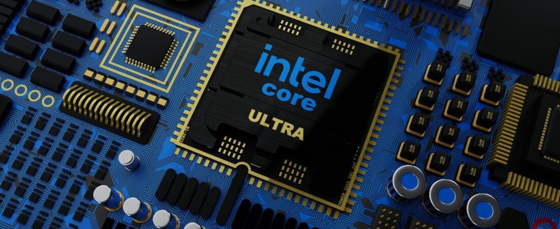
The work spans both front-end and back-of-line advances, including interconnect scaling, and covers advanced packaging for Foveros-based 3D stacking — the technology that stacks and connects chiplets. Applied says the goal is higher interconnect density, improved power delivery and better thermal performance for high-performance compute platforms designed to run agentic AI workloads.
The EPIC Center behind it
The facility giving the collaboration its shape is new. Applied announced the EPIC (Equipment and Process Innovation and Commercialization) Center in May 2023 and unveiled it in Sunnyvale on 12 October 2026. Applied describes it as the largest-ever US investment in advanced semiconductor equipment R&D, with capital spending expected to scale to about $5 billion, a 600,000-square-foot building and roughly four acres of cleanroom space.
Its model is the interesting part. Traditionally, materials research, equipment and process development, and pilot production happen in separate environments, with a handoff at each stage. EPIC puts the people who invent materials, build the equipment and make the chips in the same building, and lets chipmakers hold dedicated space inside an equipment supplier’s R&D fab — access that would otherwise come months or years later at their own sites.
Removes the Handoffs
The premise — that co-locating materials research, equipment development and pilot production removes the handoffs that add years to a chip’s journey — is a direct bet on process speed over process secrecy. Intel is one of five founding partners, alongside TSMC, Samsung Electronics, Micron and SK hynix. Innovation partners include Broadcom, Advantest, SCREEN, KIOXIA and Besi; research partners include Arizona State University, Rensselaer Polytechnic Institute, Stanford, UC Berkeley and UCLA. That roster matters for reading the announcement: the Applied–Intel collaboration is a deepening of an existing relationship, not an exclusive alliance.
Applied’s chief executive has said the technologies the AI era demands are too complex for any one company to invent alone, and EPIC rests on that premise. The partner list tells a story of its own. With TSMC, Intel, Samsung, Micron and SK hynix all founding partners, EPIC is a meeting point for competitors who rarely share a bench. That is the model’s gamble: that the shared benefit of faster materials development outweighs the risk of working near rivals.
Why packaging is the bottleneck
The collaboration’s focus on packaging reflects where the constraints now sit. As transistor scaling delivers smaller gains at each node, AI accelerators increasingly win or lose on how tightly they stack and connect dies — bandwidth between chiplets, power delivery through the stack, and heat removal from a denser package. Intel’s Foveros Direct 3D uses direct copper-to-copper hybrid bonding to achieve sub-10-micron pitch, up to ten times finer interconnect density than conventional microbump technology, enabling true vertical die stacking.
Applied’s role is in the materials and process steps that make such bonding reliable at volume. That is the heart of the matter. A modern AI accelerator is rarely one monolithic die; it is several chiplets, each built on the process that suits it, bonded into a single package. The tighter those bonds, the more bandwidth moves between compute and memory, and the less power is lost in transit. Foveros Direct 3D’s sub-10-micron pitch is a measure of how far that has come: the interconnects are now fine enough that the package behaves more like one chip than a set of parts. Advanced packaging, in other words, is where the system-level gains now come from, and materials companies sit at its foundation. The manufacturing challenge is equally real.
Hybrid bonding requires surfaces flat and clean enough that copper pads fuse directly, at pitches where a stray particle ends the die. Scaling that from a lab demonstration to millions of packages is a materials and process problem before it is a design one — which is why an equipment maker, not a chip designer, is the partner that matters here. The collaboration’s logic follows from that: Intel brings the package architecture and the volume, Applied brings the tools and the materials science, and EPIC is the room where the two meet.
Strategic Battleground
That is why “advanced packaging” has moved from a back-end afterthought to a strategic battleground. Intel has framed US advanced packaging as central to next-generation AI semiconductors, and its EMIB-T packaging is set for a fab rollout. The Applied–Intel work targets the same problem from the materials side: better deposition, bonding and interconnect processes that let stacked designs reach high-volume manufacturing. For AI chips, the practical effect of a breakthrough here is not a faster transistor but a package that moves more data with less power — often the difference between a competitive accelerator and an also-ran.
The wider reshoring context
The collaboration also fits a policy moment. Applied’s EPIC investment was contingent on support under the CHIPS and Science Act, and the center will engage with a future US National Semiconductor Technology Center. Extending the work to Intel’s Hillsboro campus, which houses Intel Foundry’s R&D, ties the equipment maker’s lab-to-fab pipeline to a chipmaker’s own development lines — a structure the US has been trying to build as it reshapes domestic semiconductor capacity.
For Intel, the collaboration is also a foundry play. Intel Foundry needs external customers to justify its capacity, and a tighter link to the equipment ecosystem is part of making its advanced packaging and process nodes attractive to them. That is a competitive necessity, not just a technical one. Intel’s foundry business is trying to win customers who currently rely on TSMC, and advanced packaging is one of the few areas where Intel has a differentiated offering — Foveros and EMIB are its own technologies, not licensed from a rival.
Applied’s semiconductor products group president, Prabu Raja, described Intel as a founding partner of EPIC and said the aim is to shorten development cycles. Intel Foundry’s Naga Chandrasekaran said the center gives the two teams an environment to work “at higher velocity.” Both are expectations about speed, and neither is a measured result.
What to watch
For the two companies, the test is whether co-location genuinely shortens development cycles — a claim the industry has made about similar centres before, and one that only shows up in how fast new process steps reach production. For the wider market, the questions are whether EPIC’s model spreads, whether the other founding partners get comparable treatment, and whether packaging advances translate into AI accelerators that ship sooner. And, for buyers of AI compute, the payoff is indirect but real: cheaper, denser packages are what make larger models economical to run.
For the industry, the broader question is whether co-innovation centres become the default way leading-edge processes are developed, or remain one equipment maker’s differentiator. Advanced packaging sits at the centre of that question because it is where the roadmaps of materials suppliers, foundries and chip designers now intersect. The unanswered question is measurement. Applied says EPIC will shorten development cycles; the industry has heard similar claims about co-location before, and the proof will be in how quickly new materials and bonding steps reach volume production at Intel and its peers.
What the announcement does and doesn’t establish
It establishes a collaboration, its technical scope and the facilities involved, and it confirms Intel’s status as an EPIC founding partner. It does not establish financial terms, deliverables, a timeline, exclusivity or any measured improvement in time-to-market. The release carries forward-looking statements, and the benefit it describes — shortening the path from lab to high-volume manufacturing — is an expectation rather than a result.
The honest summary is that two long-standing partners have formalised their work inside a facility built to remove the handoffs that slow chip development, aimed squarely at the packaging and interconnect problems that now limit AI compute. The model is credible and the facility is real; the announcement is a statement of intent, and the outcomes are years from being measurable. For advanced packaging, that timeline is the whole story — and the work that will determine it starts now, node by node.